The dynamic development of semiconductor materials
2008-08-20
The dynamic development of semiconductor materials  Whereas polymers are highly visible engineering materials with a major impact on contemporary society, semiconductors are relatively invisible but have a comparable social impact. You can find semiconductors at the heart of microprocessor chips as well as transistors. Anything that's computerized or uses radio waves depends on semiconductors. Semiconductor materials were studied in laboratories as early as 1830. The first materials studied were a group of elements and compounds that were usually poor conductors if heated. Shining light on some of them would generate an electrical current that could pass through them in one direction only. By 1874, electricity was being used not only to carry power, but to carry information. The telegraph, telephone, and later the radio were the earliest devices in an industry that would eventually be called electronics. Radio receivers required a device called a rectifier to detect signals. Ferdinand Braun used the rectifying properties of the galena crystal, a semiconductor material composed of lead sulfide, to create the cat's whisker diode for this purpose. Thus was born the first semiconductor device. Today, most semiconductor chips and transistors are created with silicon. You may have heard expressions like "Silicon Valley" and the "silicon economy," and that's why -- silicon is the heart of any electronic device. Silicon is a very common element -- for example, it is the main element in sand and quartz. If you look "silicon" up in the periodic table, you will find that it sits next to aluminum, below carbon and above germanium.
 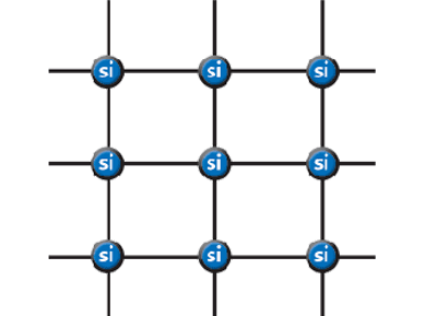 Carbon, silicon and germanium (germanium, like silicon, is also a semiconductor) have a unique property in their electron structure -- each has four electrons in its outer orbital. This allows them to form nice crystals. The four electrons form perfect covalent bonds with four neighboring atoms, creating a lattice. In carbon, we know the crystalline form as diamond. In silicon, the crystalline form is a silvery, metallic-looking substance. But as developments in new technology continue to drive a variety of sectors, high-technology manufacturing continues to represent both a vital market for trade and a serious threat for the environment. Producers of semiconductors have increasingly come into conflict with local activist groups and various regulatory bodies on the subject of environmentally safe, high technology manufacturing processes. These high-tech manufacturing processes pose a serious threat to many aspects of the local environment, as shown in the Fairchild Semiconductor case and the pollution of the local environment. High rates of birth defects, miscarriage, and cancer create a moderate urgency to resolve these kinds of problems. Production of 264,000 thousand metric tons of hazardous waste a year by all industry indicates the severity of such problems. Pollution of drinking water occurred as a result of contamination by inadequate liquid waste disposal, including acids, cyanide compounds, organic solvents, silicon tetrachloride, and arsine gas. General habitat problems, resulting from pollution of ground water, are bound to occur, affecting all species. As one of the most polymers of the silicon, Fairchild Semiconductor was required to assume the cost of clean-up and to comply with more stringent new regulations on waste storage. Semiconductor manufacturers have been assiduously searching for cleaner alternatives to present microchip production processes.
.jpg)
 New materials are often essential to new technology, but a sound basic understanding of new and old materials is even more important. We are gaining such an understanding by combining theoretical research with experimental research. Nanotechnology is increasingly dynamic, mutated by biology, surface science, materials and countless other subjects. This convergence is natural because, at the nanoscale, differences between chemistry, materials, physics and engineering fade like echoes — everything works with atoms and molecules.
  The semiconductor industry's experience with nanotechnology is not new. Companies like IBM and Intel are in production at the 90 nm node, working toward 63 nm, and eyeing 15 nm — all falling within the common definition of nanotechnology. And at the same time, many researchers are also trying to put the Nanotechnology in to the applicator of the semiconductors, which will solve a lot of the environment problems and cut down cost at the same time.