A high performance required for Transistors
2008-08-19
A high performance required for Transistors In the analog world of continuously varying signals, a transistor is a device used to amplify its electrical input. It was invented by three scientists (Walter Houser Brattain, John Bardeen, and William Shockley) at the Bell Laboratories in 1947, rapidly replaced the vacuum tube as an electronic signal regulator. 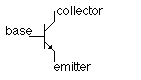 Transistors are composed of three parts – a base, a collector, and an emitter. The base is the gate controller device for the larger electrical supply. The collector is the larger electrical supply, and the emitter is the outlet for that supply. By sending varying levels of current from the base, the amount of current flowing through the gate from the collector may be regulated. In this way, a very small amount of current may be used to control a large amount of current, as in an amplifier. The same process is used to create the binary code for the digital processors but in this case a voltage threshold of five volts is needed to open the collector gate. In this way, the transistor is being used as a switch with a binary function: five volts – ON, less than five volts – OFF. Semi-conductive materials are what make the transistor possible. Most people are familiar with electrically conductive and non-conductive materials. Metals are typically thought of as being conductive. Materials such as wood, plastics, glass and ceramics are non-conductive, or insulators. In the late 1940’s a team of scientists working at Bell Labs in New Jersey, discovered how to take certain types of crystals and use them as electronic control devices by exploiting their semi-conductive properties. Most non-metallic crystalline structures would typically be considered insulators. But by forcing crystals of germanium or silicon to grow with impurities such as boron or phosphorus, the crystals gain entirely different electrical conductive properties. Generally germanium and silicon are the main material to make transistors, but compare the two materials; you could also realize their different. But because the cost of the silicon transistor is much cheaper than the germanium transistor, but also silicon transistor have faster switching properties and are far more resistant to damage by heat. So Silicon transistor has a much wider applications.
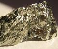
 Germanium element germanium transistor
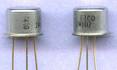
 Silicon element silicon transistor At present, though silicon transistor is only have commonly performance, but high performance transistors are only available in crystalline materials which are expensive and have to be attached ex-situ onto larger area substrates, which adds to the expense and complexity of system design. If both the electronics and display substrates can be integrated onto one platform, it would usher a new dawn in immersive and personal electronics. Individuals will thus be able to communicate, send and receive information of value, and access data about their current environment and health status with freedom, at leisure, and in comfort. However, in general, the deposition of semiconductor films used to make transistors on such substrates has to be carried out at low temperatures to preserve substrate integrity. As a result, the quality of the organic or inorganic semiconductor films is severely constrained, and has a dramatic influence on the transistor performance.
Science Daily (May 6, 2008) — The Holy Grail for transistor designers has been the requirement to be able to get high performance at reduced costs over very large substrate areas. Engineers now propose the use of clever transistor structure designs to overcome some of the issues with obtaining suitably low power and high speed operations in standard material systems. Compared to a field-effect transistor, the SGTs can operate with very short source-drain separations even with a thick gate insulator layer to achieve high speed, good stability and superior control of current uniformity, providing a significant advantage in terms of the fabrication process. Engineering of the transistor structure itself rather than the channel material can lead to improved device performance. It will enable the design of high-performance large area circuits and systems based on low-cost reliable material processes. Professor Ravi Silva, Director of the Advanced Technology Institute states: "This work will help extend the already well established CMOS fabrication technologies for use in large area applications such as displays and sensors, which are at the heart of consumer electronics. The ATI is fortunate that we have been at the forefront of two potential technologies that can lead to enhanced device performance in disordered materials by clever nano-scale structural design of disordered transistors. This type of work forms the bedrock for future electronic technologies.