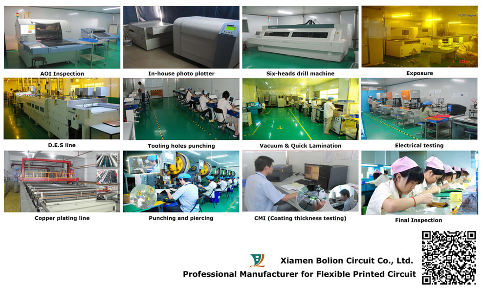
| Xiamen BOLION Workshop Capability |
| Material Cutting |
| Content | Normal | Special |
| Max dimension of material cutting | 250MM× 450MM | 250MM× 10000MM |
| Min dimension of material cutting | 250MM× 100MM |
|
| Auto-machine cutting tolerance | ± 1MM |
|
| Manually cutting tolerance | ± 2MM |
|
| Mechanical Drilling |
| Content | Normal | Special |
| Min drill Dia. | Dia. 0.20MM | Dia. 0.15MM |
| Max drill Dia. | Dia. 6.35MM |
|
| Min drill space | 0.15MM | 0.125MM |
| Drill hole Dia. tolerance | ± 0.05 MM |
|
| Laser Drilling |
| Content | Normal | Special |
| Min drill Dia. | Dia. 0.15MM | Dia. 0.1MM |
| Max drill Dia. | Dia. 6.35MM |
|
| Min drill space | 0.1MM |
|
| Drill hole Dia. tolerance | ± 0.02 MM |
|
| Copper plating |
| Content | Normal | Special |
| Copper plating capacity(thickness of hole plating) | 8-15um; 20-30 um (± 5um' s distribution) | 30-70 um |
| Max PNL dimension for PTH | 250MM× 350MM | 250MM× 2000MM |
| Aspect ratio (= board thickness / min via diameter) | 2 max for 0.10 mm vias | 3 max for 0.10 mm vias |
| 4 max for 0.15 mm vias | 5 max for 0.15 mm vias |
| 6 max for 0.20 mm vias | 7 max for 0.20 mm vias |
| 8 max for 0.25 mm vias | 9 max for 0.25 mm vias |
| Blue photosensitive etching-resist ink (Silkscreen) |
| Content | Normal | Special |
| Max PNL dimension of screen printer | 300× 450MM | 250MM× 2000MM |
| Thickness of photo image ink | 15-20um | 10-40um |
| Dry film |
| Content | Normal | Special |
| Max production dimension of dry film | 250MM× 350MM | 330MM× ∞ MM |
| Thickness of dry film | 30um | 20um; 40um; 50um |
| Exposure |
| Content | Normal | Special |
| Space between pads and line (panel plating) | ≥ 0.15MM | ≥ 0.10MM |
| Space between pads and line (via pads pattern plating) | ≥ 0.30MM | ≥ 0.20MM |
| Layer to layer misregistration tollerance | 0.2MM | 0.10MM |
| Min size of square solder mask opening | 0.40MM× 0.40MM |
|
| Min circular solder mask open size | Dia. 0.35MM |
|
| Min width of solder mask | 0.15MM | 0.10MM |
| Solder mask bridge aspect ratio (=length/width) | 10 max for 0.10 mm width | 15 max for 0.10 mm width |
| 15 max for 0.15 mm width | 20 max for 0.15 mm width |
| 20 max for 0.20 mm width | 25 max for 0.20 mm width |
| Space between solder mask open and trace | 0.1mm | 0.05mm |
| Max PNL size on exposure machine | 250MM× 350MM | 600MM× 750MM; 600MM× 10000MM (Space > 0.3MM) |
| Min dimension of non-PTH circular pad | Dia. 0.3MM | Dia. 0.2MM |
| Min anular ring width of PTH pad | 0.125MM | 0.10MM |
| Etching |
| Content | Common | Special |
| Max production size of etching | 250MM× 350MM | 500MM× ∞ |
| Min trace & space width | 0.06± 0.01 MM (copper thickness: 12 um) | 0.05± 0.01 MM (copper thickness: 12 um) |
| 0.075± 0.015 MM (copper thickness: 18 um) | 0.065± 0.015 MM (copper thickness: 18 um) |
| 0.1± 0.02 MM (copper thickness: 25~35 um) | 0.085± 0.02 MM (copper thickness: 25~35 um) |
| 0.1± 0.03 MM (copper thickness: 35~45 um) | 0.085± 0.02 MM (copper thickness: 25~35 um) |
| Coverlay alignment |
| Content | Normal | Special |
| Coverlay alignment tolerance | ± 0.30 MM (manually operating) | ± 0.20 MM |
| ± 0.20 MM (fixturally operating) | ± 0.0.15 MM |
| Min space between opening and pad | 0.2MM | 0.15MM |
| Overlap of coverlay opening and iland finger or pads | 0.5 MM | 0.3 MM for Circular pads |
| Lamination |
| Content | Normal | Special |
| PNL size on quick press | 250MM× 400 MM | 340MM× 5000MM |
| PNL size on traditional vacuum press | 630× 550MM |
|
| Adhesive squeeze when laminating | Quick press: 6± 2mil |
|
| Vacuum press: 3± 1mil |
|
| Silkscreen |
| Content | Normal | Special |
| Legend ink color | white, black | Per request |
| solder mask color | Yellow, green, amber | Per request |
| silver/carbon pastes color | silver pastes: silver; carbon pastes: black |
|
| Working size of silkscreen table | 350 MM× 700 MM | 250MM× 2000MM |
| Min character width | 0.125 MM | 0.10 MM |
| Min character height | 0.80 MM | 0.70 MM |
| Space between character and pad opening | 0.5 MM | 0.3 MM |
| Silkscreen alignment tolerance | ± 0.30MM | ± 0.20 MM |
| Silkscreen silver pastes tolerance | ± 0.50MM | ± 0.40 MM |
| Silkscreen solder mask tolerance | ± 0.50MM | ± 0.30 MM |
| Min distance between silkscreen to outline | 0.3 MM |
|
| Min distance between silkscreen to NPTH | 0.3 MM |
|
| Printed ink thickness | Legend character: 8-15 um |
|
| Solder mask: 15-25 um |
|
| Silver ink: 10~25 um |
|
| Carbon ink: 10-20um |
|
| Carbon ink: 10-20um |
|
| Final finshing |
| Content | Normal coating thickness | Normal PNL size |
| Plating nickel gold (In house) | Ni: 2-9um; Au: 0.03-0.09um | 300mm× 400 MM |
| Plating hard gold (In house) | Ni: 2-9um; Au: 0.1-1.0um | 300mm× 400 MM |
| Plating soft gold (In house) | Ni: 2-9um; Au: 0.03-0.09um | 300mm× 400 MM |
| Plating pure tin (In house) | 2.0-8.0um | 300mm× 400 MM |
| Immersion Tin (In house) | 0.3-0.6um | 300mm× 400 MM |
| OSP (In house) | N/A | 300mm× 400 MM |
| ENIG (Hard Nickel) (In house) | Ni: 2-6um; Au: 0.03-0.10um | 300mm× 400 MM |
| ENIG (Soft Nickel) (In house) | Ni: 2-6um; Au: 0.03-0.10um | 300mm× 400 MM |
| ENEPIG (Hard Nickel) (In house) | Ni: 2-6um; Au: 0.03-0.10um | 300mm× 400 MM |
| HASL (Outsource) | Cover the pads with min thickness 1~2 um | 300mm× 400 MM |
| Immersion silver (Outsource) | Per standand creteria | 300mm× 400 MM |
| Electrical test (Flying probe tester for sample) |
| Content | Normal | Special |
| Max test points qty | 4096 |
|
| Min probe | 0.25MM | 0.15MM |
| Max probe | 1.70MM |
|
| Safe distance between test probes | 0.20MM |
|
| Stiffener, PSA alignment tolerance |
| Content | Normal | Special |
| Min safe space between alignments and pads opening | ± 0.50 MM | ± 0.30 MM |
| Tolerance without hole-centered alignments | ± 0.40 MM | ± 0.40 MM |
| Tolerance with hole-centered alignments | ± 0.2 MM |
|
| Min strip width of PSA | 2MM | 1.0 MM |
| Min seperate PSA size | 13× 2.0 MM |
|
| Die cutting |
| Content | Normal | Special |
| Outline manually cutting (Outline length≤ 100MM) | ± 0.20 MM (Need manually cut guide line) |
|
| Outline manually cut (Outline length > 100MM) | ± 2 ‰ |
|
| Outline soft tooling cut (Outline length≤ 100MM) | ± 0.20 MM |
|
| Outline soft tooling cut (Outline length > 100MM) | ± 2‰ |
|
| Outline etching die cut (Outline length≤ 100MM) | ± 0.10 MM |
|
| Outline etching die cut (Outline length > 100MM) | ± 1.5‰ |
|
| Outline normal hard tooling cut (L< 100MM) | ± 0.10 MM |
|
| Outline normal hard tooling cut (100≤ L< 150MM) | ± 0.15 MM |
|
| Outline normal hard toolingcut (L≥ 150MM) | ± 1.5‰ | ± 1.3‰ |
| Outline precise hard tooling cut (L< 100MM) | ± 0.05 MM |
|
| Outline precise hard tooling cut (100≤ L< 150MM) | ± 0.1 MM |
|
| Outline precise hard toolingcut (L≥ 150MM) | ± 1.2‰ | ± 1.0‰ |
| Outline segmented cut | ± 1.5‰ (soft tooling) |
|
| Min punching hole Dia. and tolerance | Dia. 0.60 ± 0.05 MM |
|
| Tolerance for hole to board edge | 1.0 MM(normal soft die cut tooling) | 0.50 MM(Etching die cut tooling, normal hard tooling) |
| Tolerance for trace center to board edge | 0.10 MM | 0.08 MM(precise hard tooling) |
| Package |
|
|
| Content | Normal | Special |
| Tray | Per product size |
|
| Low viscosity PET layer | 300× 210MM |
|
| Ziplock bag | Per product size |
|
| Vacuum sealing package | 16cmx23cm, 20cmx34cm, | 28cmx36cm, 30cmx50cm |


