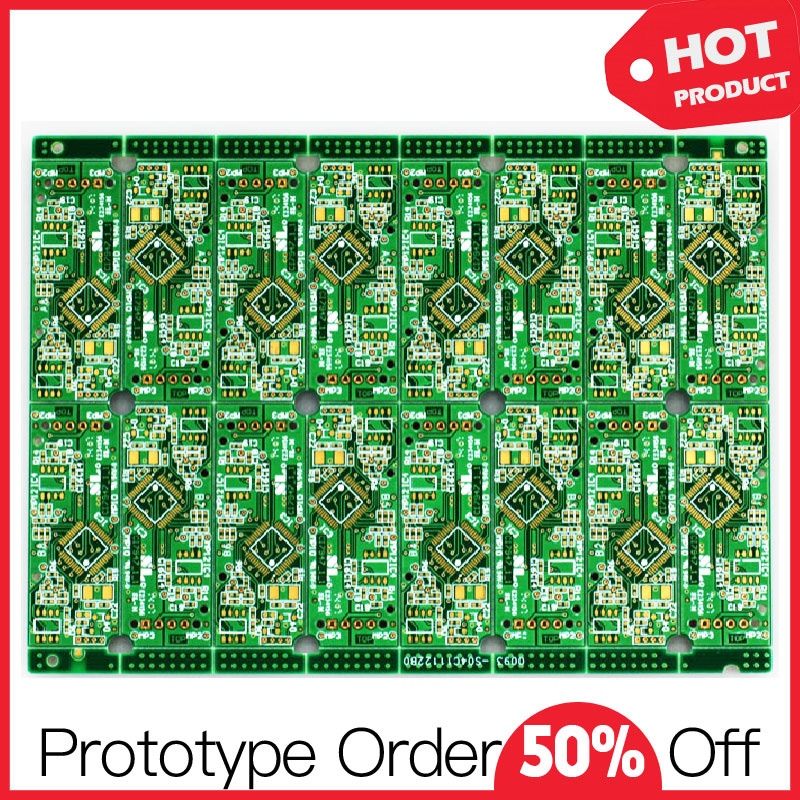
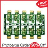
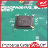
Reliable Multilayer Fr4 Printed Circuit Board with UL
| Price: |
US $ 0.29-0.45/Piece |
| Min Order: |
1/Piece |
| Pay Type: |
L/C,T/T,Western Union |
| Type: |
Combining Rigid Circuit Board |
| Dielectric: |
FR-4 |
| Material: |
Fiberglass Epoxy Resin + Polyimide Resin |
| Flame Retardant Properties: |
HB |
Product Description
Reliable Multilayer Fr4 Printed Circuit Board with UL
Our Multilayer Printed Circuit Board Manufacturing Description| Specifications | Technology |
| Number of Layers | 1-12Layers |
| Board Materials | FR4 (Tg - 135C, 145C, 170C)
Rogers Ultralam 2000
Rogers RO4350
Rogers RO4003
Polyimide
Teflon
Black FR4
Arlon AR350
Getek Copper Clad Thermal Substrates
Hybrid (Rogers and FR4) BT Epoxy
Nelco 4013
Metal Core Materials |
| Stiffeners | Thermo Set and PSA Based Aluminium
FR4
Stainless Steel
Polymide |
| Final PCB Thickness | 2 Layer - Min .005" Max .250"
4 Layer - Min .015" Max .250"
6 Layer - Min .025" Max .250"
8 Layer - Min .031" Max .250"
10 Layer - Min .040" Max .250"
12 Layer - Min .047" Max .250" |
| Core Thickness | Min .0025" |
| Maximum PCB Size | 2 Layer 20" x 28" |
| Mulitlayer 16" x 26" |
| Minimum Conductor Space | 0.003" |
| Minimum Conductor Width | 0.003" |
| Minimum Drill Hole Size | 0.006" |
| Finish Plating / Surface Finishes | HASL - Leaded Solder Tin/Nickel
HASL - Lead Free Solder
Electroless Soft Gold
Wire Bondable Soft Gold
Nickel Flash Gold
Electroless Nickel
Immersion Gold OSP
Electrolytic Nickel /Hard Gold and Selective Gold
Immersion Silver
Immersion Tin
Carbon Ink
ENIG |
| Finished Copper - Outer Layers | 1oz Cu - Min .004" Trace/Space
2oz Cu - Min .005" Trace Space
3oz Cu - Min .008" Trace/Space
4oz Cu - Min .010" Trace/Space
5oz Cu - Min .012" Trace/Space |
| Finished Copper - Inner Layers | 0.5oz Cu - Min .004" Trace/Space
1oz Cu - Min .005" Trace/Space
2oz Cu - Min .006" Trace/Space
3oz Cu - Min .010" Trace/Space
4oz Cu - Min .012" Trace/Space |
| Inner Layer Clearances | Min .008"
Minimum Finished Hole Size
Final Thickness <=.062" - .006' Hole Final Thickness .150" - .014" Hole
Final Thickness .093" - .010" Hole Final Thickness .200" - .018" Hole
Final Thickness .125" - .012" Hole Final Thickness .250" - .020" Hole |
| Gold Fingers | 1 to 4 edges |
| Solder Mask Type | Per IPC-SM-840
LPI Soldermask
Peelable Soldermask |
| Solder Mask Colors | Green/Green
Matte White
Black/Black
Matte Clear
Blue Top and Bottom Mix
Red One or Both Sides Mix |
| Silkscreen Type | Thermal Cure Epoxy Ink
LPI Ink |
| Silkscreen Colors | White
Black
Yellow Top and Bottom Mix
Red One or Both Sides Mix
Blue |
| CNC Functions | Scoring Edge to Edge Plated Counter bores
Skip Scoring - .250" Spacing Milling
30 or 60 Degree Score Angle Blind and Buried Vias
30 to 100 Degree Countersink Controlled Z Axis Route
15 to 45 Degree Gold Finger Bevel Castellated Barrels
Counterbores Offset or Recessed Beveling
Plated Countersinks |
| Other PCB Services | Blind and Buried Vias
Plated Slots Specified Dielectric
Tented Vias Controlled Impedance
Solder mask Plugged Vias Via Caps (Solder Mask)
Conductive Filled Vias |
| Quality / Testing | Inspect to IPC Class III Continuity Resistance - 10 to 20 Ohms
Net List Test per IPC-356D Isolation Resistance - 2 to 30 Megaohms
Test Voltage - 100 to 250 Volts Minimum SMT Pitch 0.5 mm |
| Tolerances | PTH Hole Size - +/- .002"
Front to Back - +/- .002"
NPTH Hole Size - +/- .001"
Solder Mask - +/- .002"
Tooling Holes - +/- .001"
Hole to Pad - +/- .005" |
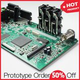
Our Multilayer Printed Circuit Board Manufacturing ProcessOur multilayer printed circuit board manufacturing capabilities can meet almost 95% demand of customer requirements and actually we concentrated on this field for decades, so plant facilities have been advanced to high level and your intelligent manufacturing could be well handled here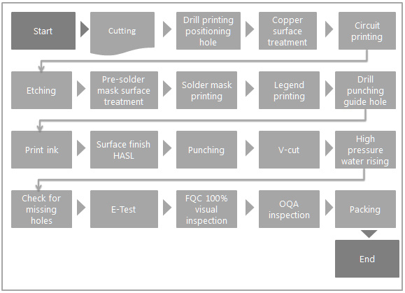 About UsAs a service-leading PCB manufacturing and PCB assembly (PCBA) partner, NOD Electronics strives to support international small-medium business with 10+ years engineering experience in Electronic Manufacturing Services (EMS). Our headquarter is located in Guangzhou, China. We have 10,000 square meters plant, 287 employees and 42 engineers, monthly capabilities of 15,000 square meters PCB design & fabrication and 80 million spot SMT. We were approved by ISO9001-2008, TS16949, UL, CE, RoHS.Our customers are widely distributed in mainland China, Taiwan, the United States, Japan, Singapore, Korea, Russia, Germany, Switzerland and other parts of the word.
 Your multilayer printed circuit board demand will be perfectly handled by our professional production line and responsible work team.
Frequently Asked Questions (FAQs)How we ensure the quality of circuit board manufacturing and assembly?We choose top sheet suppliers to ensure stable performance (general FR-4). During the manufacturing process, automatic copper plating lines and high-speed drilling machines (brand:TMAX) to make accuracy and fast delivery guaranteed. All printed circuit board will be detected by advanced automatic flying probe machines (or test frame ) at subsequent stages to make sure each PCB is OK from inner circuits to outside shape. How long will you get our quotation of PCB manufacturing and assembly?In general, PCB sample is delivered in 24~72 hours (urgent order less than 24 hours). Volume production can be completed in 7 working days. If for subsequent PCB assembly and test requirements, the lead time could be less than 15 days. What kind of files you have to send us to get quotation?You have to send us PCB design files (gerbers or .pcb acceptable), Bill of Materials (BOM), Quantities to make quote and other technical requirements (.step/.txt/.xls files acceptable) What payment methods we can support?We accept T/T, L/C, West Union as payment methods. For prototype order, you have to make 100% payment in advance, but for mass production 70% payment in advance and 30% payment before delivery. What measures we take to avoid counterfeit components?Procurement only from manufacturer or big general agentOriginal quality certificate of component can be issued (if necessary)Inspections of shape, silkscreen and conductivity attributes in incoming quality controlStrong responsibilities and perspectives of long-term relationship What measures we take to protect clients IP and confidentiality?Sign NDA (Non-disclosure Agreement)Using number code in stead of client name during manufacturing processSeparate assembly workshop and taking photo is NOT allowedDocuments of engineering process are archived and reserved
As a service-leading PCB manufacturing and PCB assembly (PCBA) partner, NOD Electronics strives to support international small-medium business with 10+ years engineering experience in Electronic Manufacturing Services (EMS). Our headquarter is located in Guangzhou, China. We have 10, 000 square meters plant, 287 employees and 42 engineers, monthly capabilities of 15, 000 square meters PCB design & fabrication and 80 million spot SMT. We were approved by ISO9001-2008, TS16949, UL, CE, RoHS.
We strive to be your rightest partner in electronic manufacturing serivce with a commitment from creative team members. Do you agree that every electronic product has its soul, bearing the designer's product concept, just like the Apples and Steve Jobs? Electronic product is a bridge between the customer and designer rather than a cold and ruthless object. Although they have no verbal communication, they have soul connection in between.
So, we perform and create a bridge, which turns your concept or design into a product and present in front of the customers by offering reliable manufacturing solutions and engineering support, including New Product Introduction (NPI), Printed Circuit Board (PCB) design, Printed Circuit Board Assembly (PCBA), Casing (plastic & mental) solutions.
More >
Other Products with This Manufacturers