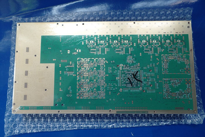
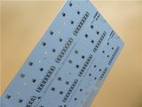
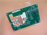
10 Layer High Frequency Circuit Board PCB RO4350b and RO4450b
| Price: |
US $ 0.98/Piece |
| Min Order: |
1/Piece |
| Pay Type: |
T/T,Western Union,Paypal |
| Prod Model: |
BIC1289R1.3 |
| Surface Finish: |
Immersion Gold |
| Solder Mask Color: |
Green |
| Board Thick: |
2.0mm |
| Legend Color: |
White |
| Out Copper Thick: |
1.5 Oz |
| Inner Copper Thick: |
0.5 Oz |
| Minimum Trace And Space: |
5.5 Mil/5 Mil |
| Minimum/Maximum Holes: |
0.3/2.0mm |
| Via: |
BGA Package |
| Test: |
100% Electrical Test |
| Type: |
Rigid Circuit Board |
| Flame Retardant Properties: |
V0 |
| Dielectric: |
RO4350b,RO4450b |
| Material: |
Hydrocarbon/Woven Glass |
| Insulation Materials: |
Glass Reinforced Hydrocarbon |
Product Description
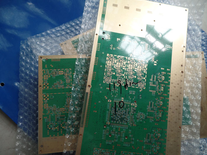
10 Layer High Frequency Circuit Board PCB RO4350B With RO4450B Applied In Broadband
Wireless Solutions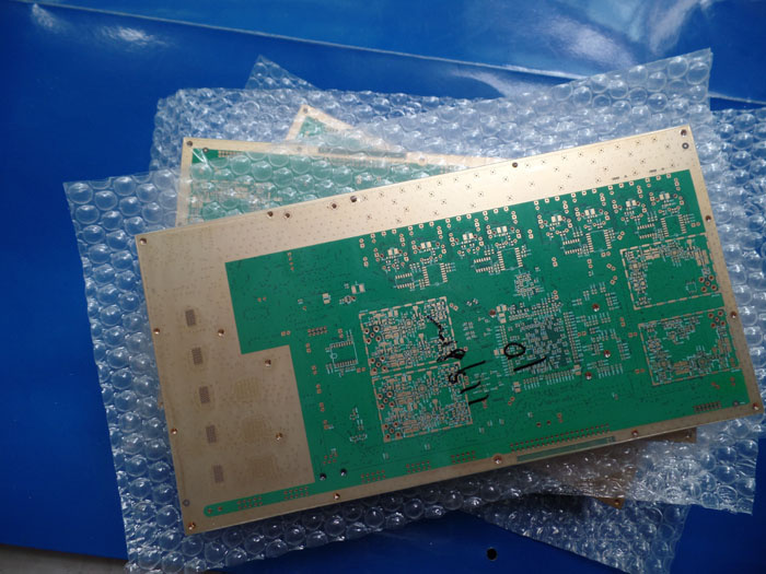 Commodity Introduction
This is a type of RO4350B and RO4450B PCB for the application of Broadband Wireless Solutions.
It's a 10 layer board at 2.0mm thick. The base laminate is from Rogers Corp.. Solder mask and
silkscreen from Taiyo. It's fabricated per IPC 6012 Class 2 using supplied Gerber data. Each 10
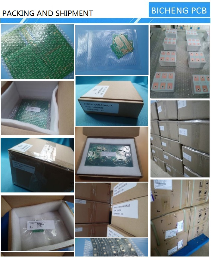
boards or panels are packed separately. 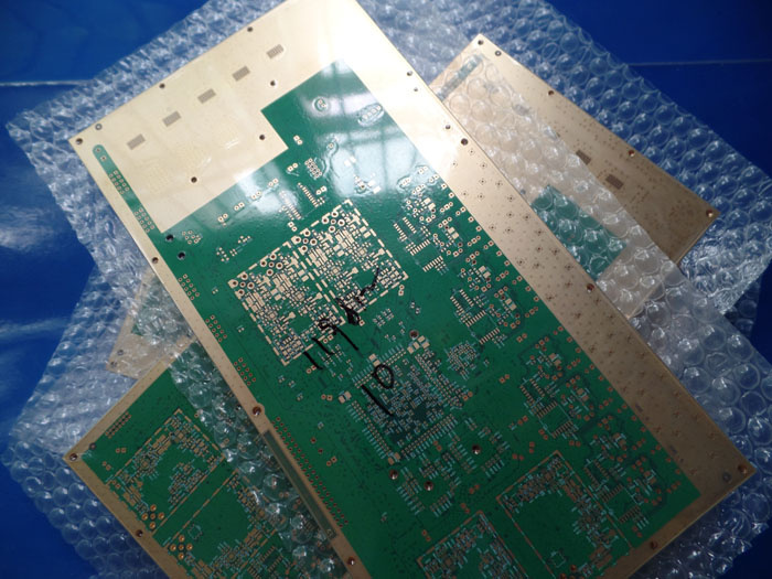 Parameters & Data Sheet
| PCB SIZE | 215 x 178mm=1PCS=1design |
| BOARD TYPE | |
| Number of Layers | Multilayer High Frequency PCB, 10 Layer PCB |
| Surface Mount Components | YES |
| Through Hole Components | NO |
| LAYER STACKUP | TOP Layer: signal - 1/2oz foil + 25μm Cu |
| Core RO4350B -0.254mm |
| INT 1: mixed - 1/2oz foil |
| Prepreg RO4450B -0.202mm (2 x 0.101) |
| INT 2: mixed - 1/2oz foil |
| Core RO4350B -0.254mm |
| INT 3: mixed - 1/2oz foil |
| Prepreg RO4450B -0.202mm (2 x 0.101) |
| INT 4: mixed - 1/2oz foil |
| Core RO4350B -0.254mm |
| INT 5: mixed - 1/2oz foil |
| Prepreg RO4450B -0.202mm (2 x 0.101) |
| INT 6: mixed - 1/2oz foil |
| Core RO4350B -0.254mm |
| INT 7: mixed - 1/2oz foil |
| Prepreg RO4450B -0.202mm (2 x 0.101) |
| INT 8: mixed - 1/2oz foil |
| Core RO4350B -0.254mm |
| BOT Layer: signal - 1/2oz foil + 25μm Cu |
| TECHNOLOGY | |
| Minimum Trace and Space: | 5.5mil/5mil |
| Minimum / Maximum Holes: | 0.3/2.0mm |
| Number of Different Holes: | 9 |
| Number of Drill Holes: | 7505 |
| Number of Milled Slots: | 0 |
| Number of Internal Cutouts: | 0 |
| Impedance Control | NO |
| BOARD MATERIAL | |
| Glass Epoxy: | RO4350B core 0.254mm(10mil),
RO4450B PP 0.1mm(4mil) |
| Final foil external: | 1oz |
| Final foil internal: | 0.5oz |
| Final height of PCB: | 2.0mm ±10% |
| PLATING AND COATING | |
| Surface Finish | Electroless nickel over Immersion Gold (ENIG)( 0.05µm over 3µm nickel) |
| Solder Mask Apply To: | Top and Bottom, 12micon Minimum. |
| Solder Mask Color: | Green, PSR-2000GT600D, Taiyo supplied. |
| Solder Mask Type: | LPSM |
| CONTOUR/CUTTING | Routing |
| MARKING | |
| Side of Component Legend | TOP |
| Colour of Component Legend | White, IJR-4000 MW300, Taiyo Supplied. |
| Manufacturer Name or Logo: | Marked on the board in a conductor and
leged FREE AREA |
| VIA | Plated Through Hole(PTH), via tented.
BGA package |
| FLAMIBILITY RATING | UL 94-V0 Approval MIN. |
| DIMENSION TOLERANCE | |
| Outline dimension: | 0.0059" (0.15mm) |
| Board plating: | 0.0030" (0.076mm) |
| Drill tolerance: | 0.002" (0.05mm) |
| TEST | 100% Electrical Test prior shipment |
| APPLICATION: | Broadband wireless solutions, Wifi Usb Dongle
Modem Router Wireless
Gsm Tracker
Antena Wireless
Bluetooth |
TYPE OF ARTWORK TO
BE SUPPLIED | email file, Gerber RS-274-X, PCBDOC etc |
| SERVICE AREA | Worldwide, Globally. |
 The components of multilayer PCB: copper foil
A multilayer board consists of copper foils, thin rigid laminates and prepreg sheets.
The standard thicknesses for copper foils are shown below| µm | 5 | 9 | 12 | 17.5 | 35 | 70 |
| oz | 0.14 | 0.25 | 0.34 | 0.5 | 1 | 2 |
Thick copper (heavy copper) foils are used for voltage and ground planes by some electronics
companies. Thicknesses up to 210 µm (6 oz) are specified for high voltage coil boards. For very
fineline boards, 5 and 9 µm (0.14 and 0.25 oz.), ultrathin copper foils are also used for the outer
layers.
Copper foils are used as copper cladding of the thin laminates used in the inner layers. Such
laminates can be delivered with different copper thicknesses on the two sides, for example,
17.5 µm (0.5 oz.) on one side for a signal layer and 35 µm (1 oz.) on the other side for ground
or voltage planes.
Copper foils are sometimes used directly as cap foils for the outer layers. In such cases, the
copper foils are bonded to the next layers by means of prepreg and form the outer layer circuits.
For signal outer layers, the copper foil thickness is usually 17.5 µm (0.5 oz.) or 35 µm (1 oz.)
depending on the minimum track width and spacing. In the case of high-density fine-line boards,
5 or 9 µm (0.14 or 0.25 oz.) ultrathin copper foils can be the only solution to achieve the required
high resolution when etching the board.
For signal inner layers, a 35 µm (1 oz.) copper foil is normally chosen. For ground and voltage
planes, 35 µm (1 oz.) and 70 µm (2 oz.) copper foils can be used. However, the thicker foil, the
more difficult it is to fill the apertures in the planes around the hole wall with epoxy flowing from
the prepreg sheets during lamination. 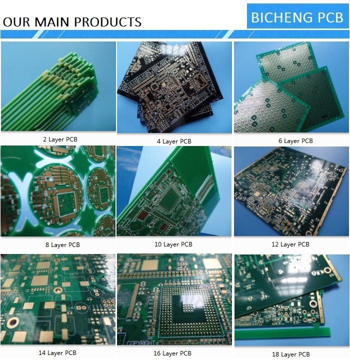

Founded in 2003, Bicheng Enterprise Limited is a professional PCB export enterprise. We have established a good relationship of cooperation with well-known enterprises in the same industry.
The factories have been ISO 9001-2008, ISO 14001-2004 and ISO/TS16949-2009 quality management system certified. Over the past 14 years, we have provided professional circuit board manufacturing solutions for more than 5000 companies worldwide.
Different plant scale to suit for your requirements
16000 square meter factory building
30000 square meter month capability
8000 types of PCB per month
ISO9001, ISO14001, TS16949, UL Certified
We have our own advantages to help you saving cost and time spent on PCB, booster your new products go to market quickly.
A) Various kinds of PCB products
Double sided PCB
Multilayer PCB up to 32 layers
FR-4 PCB (Tg130, Tg170)
High frequency PCB (RO4350B, RO4003C)
Aluminum PCB (1W/MK, 2W/MK, 3W/MK)
Flexible PCB
HDI PCB Board
B) Multiple PCB technology to meet the market demands
Blind via PCB, Via in pad PCB, Fine pitch BGA PCB
Impedance controlled PCB
Heavy copper PCB
Hybrid material PCB
C) Many discount policies for new customers
SMT stencil foil, free of charge
Prototype shipping cost, free of charge
Prototype test, free of charge
PCB panelization, free of charge
D) High quality PCB services
Engineering design prevents problems from occurring in pre-production.
Meet your PCB needs from prototype to mass volume production.
Eligible products rate of first production: >95%
Delivery on time: >98%, door to door shipment service
Customer complaint rate: <1%
Choose BichengPCB means you choose hassle free.
More >
Other Products with This Manufacturers