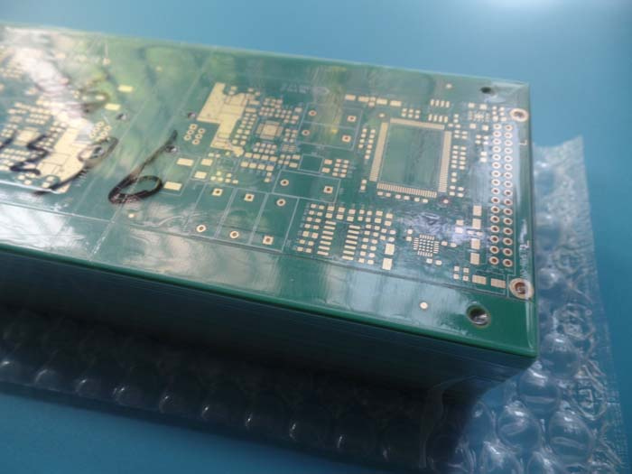
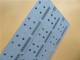
Fr-4 Multilayer 6 Layer PCB Board with Immersion Gold
| Price: |
US $ 0.76/Piece |
| Min Order: |
1/Piece |
| Pay Type: |
T/T,Western Union,Paypal |
| Prod Model: |
BIC-258-V2.58 |
| Inner Layer Cu Thickness: |
1 Oz |
| Pth Cu Thickness: |
22.3 Um |
| Surface Cu Thickness: |
35.5 Um |
| Finished Thickness: |
1.62mm |
| Surface Treatment: |
Enig |
| Solder Mask: |
Green, Nan Ya, Lp-4G G-05 |
| Legend: |
White, Tai Yo, S-380W |
| Trace Width (mm): |
0.255mm |
| Spacing (mm): |
0.376mm |
| Warp And Twist: |
0.21% |
| Type: |
Rigid Circuit Board |
| Dielectric: |
FR-4 |
| Material: |
Fiberglass Epoxy |
| Flame Retardant Properties: |
V0 |
Product Description
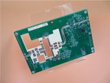
Multilayer PCB High Tg170 FR-4 6 Layer with Green Solder Mask and Gold for Codec
Application
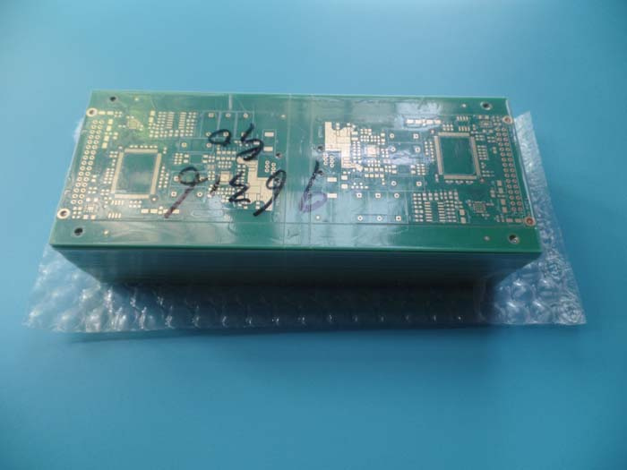
Commodity Introduction This is a type of FR-4 PCB for the application of Codec Application. It's a 6 layer board at 1.6mm
thick. The base laminate is from ShengYi, Solder mask and silkscreen from Nan Ya and Taiyo. It's
fabricated per IPC 6012 Class 2 using supplied Gerber data. Each 10 boards or panels are packed
separately.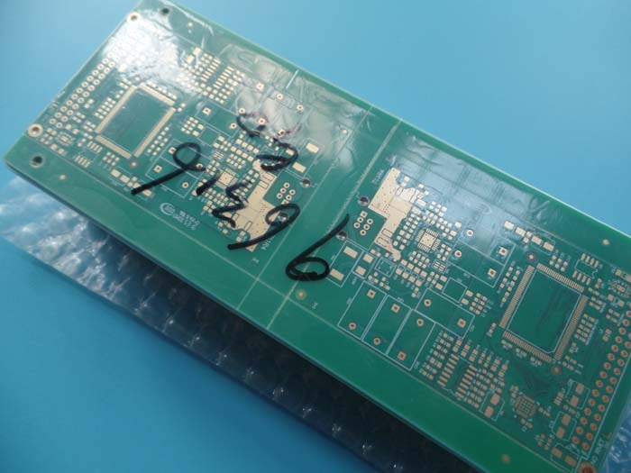 Parameters & Data Sheet
| Item | Description | Requirement | Actual |
| Laminate | Laminate Type | FR4 | FR4 |
| Supplier | SHENGYI | SHENGYI |
| Tg | TG 170 | TG 170 |
| Finished thickness | 1.57+/--0.15 mm | 1.62 mm |
| Plating Thickness | PTH Cu thickness | 20 um | 22.3 um |
| Inner layer Cu Thickness | 35 um | 35 um |
| Surface Cu thickness | 35 um | 35.5 um |
| Solder Mask | Material type | LP-4G G-05 | LP-4G G-05 |
| Supplier | Nan Ya | Nan Ya |
| Color | Green | Green |
| Single / both sides | Both Sides | Both Sides |
| S/M thickness | >= 10.0 um | 28.73 um |
| 3M tape test | NO Peel Off | no peel off |
| Legend | Material type | S-380W | S-380w |
| Supplier | Tai yo | Tai yo |
| Color | White | White |
| Location | CS | CS |
| 3M tape test | No peel off | no peel off |
| Circuit | Trace Width (mm) | 0.25+/-20%mm | 0.255mm |
| Spacing (mm) | 0.38+/- 20%mm | 0.376 mm |
| Identification | UL mark | 94V-0 | 94V-0 |
| Company Logo | QM | QM |
| Date code | 1017 | 1017 |
| Mark location | CS | CS |
| Surface Treatment | ENIG | Nickel | 100 u" | 134.6 u" |
| Gold | 1.2 u" | 1.28 u" |
| Reliabilty Tests | Thermal shock test | 288±5ºC,10sec,
3 cycles | NO Discolor,
NO Delamination |
| solder abllity test | 235±5ºC, | 100% wetting |
| Function | Electrioal Test | 100% | pass |
| Standard | IPC-A 600H class 2,
IPC_6012C CLASS 2 | | 100% | Pass |
| Appearance | Visual inspection | 100% | Pass |
| warp and twist | <= 0.75% | 0.21% |
| Others | V-Cut thickness | 0.4±0.1mm | 0.39mm |
| Angle | 30+/- 5 | 30º |
 Finished dimension (unit: mm): including v-cut
| No | Required | Actual Dimension |
| 1 | 128 | 127.94 | 127.87 | 127.94 | 127.96 | 12794 |
| 2 | 190 | 189.95 | 189.89 | 189.96 | 189.96 | 189.95 |
Hole size and slot dimension(unit: mm, PTH tolerance +/-0.076, NPTH +/-0.05mm)| No | Required | PTH/NPTH | Actual Dimension |
| 1 | 0.9 | Y | 0.975 | 0.925 | 0.900 | 0.000 |
| 2 | 1.02 | Y | 1.075 | 1.000 | 0.975 | 1.050 |
| 3 | 1.3 | Y | 1.300 | 1.375 | 1.325 | 1.300 |
| 4 | 3.05 | Y | 3.050 | 3.050 | 2.975 | 3.100 |
| 5 | 3.5 | N | 3.475 | 3.550 | 3.450 | 3.550 |
Learn PCB and Buy PCB
Image Transfer
As PCBs become more complex, patterns (pads and tracks) are becoming finer and finer. It is very
crucial to transfer the image without any noticeable distortion. The finished image will act as
a plating resist. This is usually based on a dry-film resist of a certain thickness that matches the
plating thickness.
The most commonly used track width is about 0.102 mm (4 mils) which could be regarded as
the standard width. However, widths of 0.076 mm (3 mils) are also in use, and some
Chinese PCB manufacturers operate with track widths down to 0.050 mm (2 mils). But the PCB
designer should not be tempted by track widths of 0.076 mm (3 mils) or smaller because
the manufacturing yield becomes lower and the board price, correspondingly, higher.
The purpose of image transfer is to cover those areas of the board that are not to be plated with
copper, tin/lead or pure tin, with a plating resist, and to leave the pattern open for electroplating.
With plated-through-hole boards, image transfer is performed by means of a photopolymer dry
-film process consists of the following steps:- Lamination
- Registration
- Exposure
- Developing
- Laser Direct Imaging

Founded in 2003, Bicheng Enterprise Limited is a professional PCB export enterprise. We have established a good relationship of cooperation with well-known enterprises in the same industry.
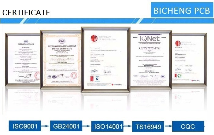
The factories have been ISO 9001-2008, ISO 14001-2004 and ISO/TS16949-2009 quality management system certified. Over the past 14 years, we have provided professional circuit board manufacturing solutions for more than 5000 companies worldwide.
Different plant scale to suit for your requirements
16000 square meter factory building
30000 square meter month capability
8000 types of PCB per month
ISO9001, ISO14001, TS16949, UL Certified
We have our own advantages to help you saving cost and time spent on PCB, booster your new products go to market quickly.
A) Various kinds of PCB products
Double sided PCB
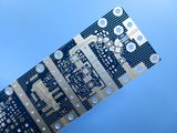
Multilayer PCB up to 32 layers
FR-4 PCB (Tg130, Tg170)
High frequency PCB (RO4350B, RO4003C)
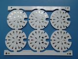
Aluminum PCB (1W/MK, 2W/MK, 3W/MK)
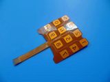
Flexible PCB
HDI PCB Board
B) Multiple PCB technology to meet the market demands
Blind via PCB, Via in pad PCB, Fine pitch BGA PCB
Impedance controlled PCB
Heavy copper PCB
Hybrid material PCB
C) Many discount policies for new customers
SMT stencil foil, free of charge
Prototype shipping cost, free of charge
Prototype test, free of charge
PCB panelization, free of charge
D) High quality PCB services
Engineering design prevents problems from occurring in pre-production.
Meet your PCB needs from prototype to mass volume production.
Eligible products rate of first production: >95%
Delivery on time: >98%, door to door shipment service
Customer complaint rate: <1%
Choose BichengPCB means you choose hassle free.
More >
Other Products with This Manufacturers