Categories
- Power Supply
- Motor
- Antenna
-
Battery and Charger
- Rechargeable Battery
- Battery Charger
- Car Battery
- Deep Cycle Battery
- Lead Acid Battery
- 6V Battery
- 9V Battery
- 12V Battery
- Lithium Battery
- Cr2 Battery
- Aa Battery
- Aaaa Battery
- Aaa Battery
- Battery Pack
- C Battery
- Agm Battery
- Nimh Battery
- Battery Booster
- Cmos Battery
- Power Battery
- Alkaline Battery
- Car Battery Charger
- Marine Battery
- Cr123A Battery
Hot Tags > - Transformer
- Gps
- Transmitter
- Capacitor
-
Variable-Frequency Drive
Hot Tags >
- Remote Control
- Fuse
-
Insulator
- Insulation Material
- Electrical Insulator
- Glass Insulator
- Porcelain Insulator
- Pin Insulator
- High Voltage Insulator
- Composite Insulator
- Ceramic Insulator
- Suspension Insulator
- Polymer Insulator
- Pin Type Insulator
- Insulated Wire
- Rubber Insulation
- Bushing Insulator
- Line Post Insulator
- Busbar Insulator
Hot Tags > - Resistor
- Inductor
-
Switch
- Automatic Transfer Switch
- Combination Switch
- Dip Switch
- Flow Switch
- Isolation Switch
- Limit Switch
- Membrane Switch
- Micro Switch
- Pressure Switch
- Push Button Switch
- Reed Switch
- Remote Control Switch
- Rocker Switch
- Rotary Switch
- Sensor Switch
- Tact Switch
- Time Switch
- Toggle Switch
- Electronic Switch
Hot Tags > -
Sensor
- Abs Sensor
- Proximity Sensor
- Acceleration Sensor
- Current Sensor
- Differential Pressure Sensor
- Displacement Sensor
- Fiber Optic Sensor
- Flow Sensor
- Gas Sensor
- Image Sensor
- Infrared Sensor
- Sensor Light
- Liquid Level Sensor
- Load Cell
- Photoelectric Sensor
- Pressure Sensor
- Temperature Sensor
- Throttle Position Sensor
- Torque Sensor
- Ultrasonic Sensor
- Voltage Sensor
- Water Leak Sensor
Hot Tags > - Terminals and Connectors
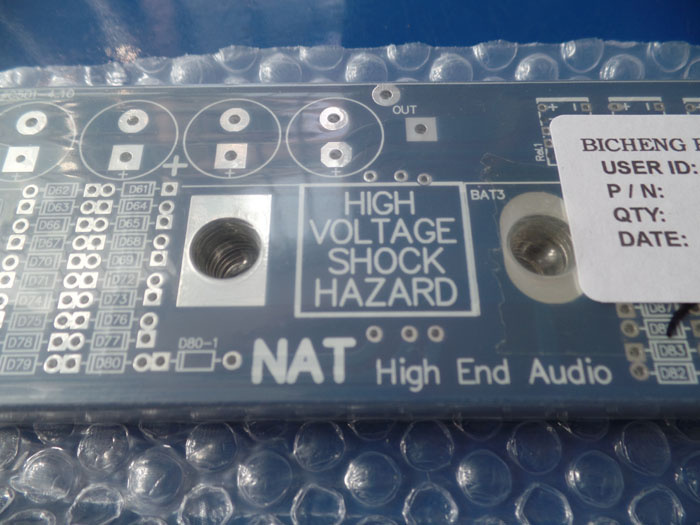
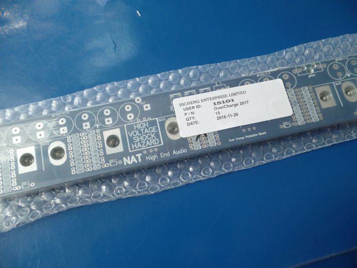
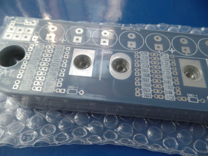
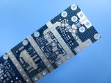
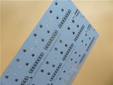
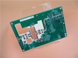
- Circuit Board
- Socket
- Plug
- Relay and Contactor
-
Other Electronic Component
Hot Tags >
- Circuit Breaker
-
Heating and Temperature Control
Hot Tags >
- Inverter
- Cable and Wire