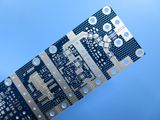
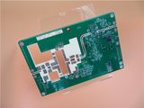
Immersion Gold PCB 4 Layer Circuit Board with 1.6mm Thick
| Price: |
US $ 0.63/Piece |
| Min Order: |
1/Piece |
| Pay Type: |
T/T,Western Union,Paypal |
| Prod Model: |
BIC-402-V4.02 |
| Board Thick: |
1.62mm |
| Surface Finish: |
Immersion Gold |
| Out Layer Copper Thickness: |
1 Oz |
| Solder Mask Color: |
Green |
| Silkscreen Color: |
White |
| Electronic Test: |
100%Passed |
| Applications1: |
DSL Modems |
| Applications2: |
ADSL Router,WiFi USB Adapter |
| Applications3: |
3G Modem,WiFi Bridge |
| Applications4: |
GSM Alarm,USB Dongle, |
| Type: |
Rigid Circuit Board |
| Dielectric: |
FR-4 |
| Material: |
Fiberglass Epoxy |
| Flame Retardant Properties: |
V0 |
Product Description
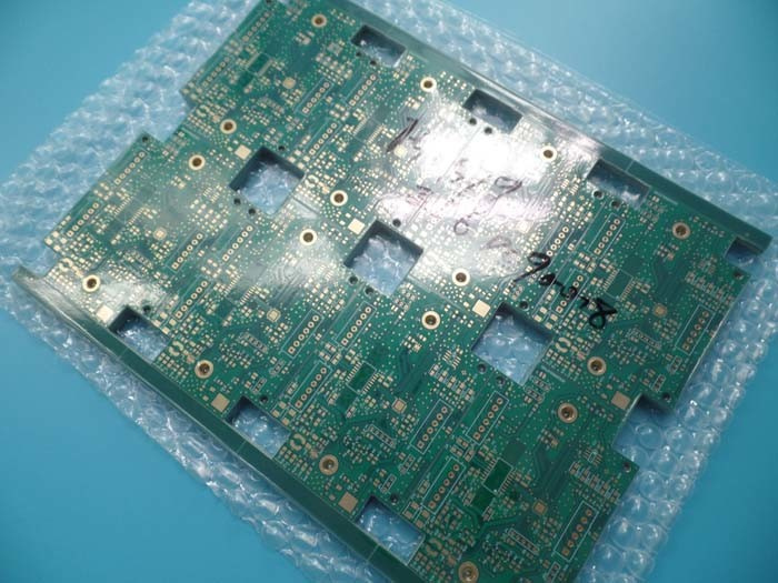
Volume Production Multilayer PCB 4 Layer Tg135 FR4 Big panel with Immersion Gold
 Commodity Introduction
This is a type of FR-4 PCB for the application of Wireless Adapter. It's a 4 layer board at 1.6mm
thick. The base laminate is from ITEQ, Solder mask and silkscreen from TaiYo. It's fabricated
per IPC 6012 Class 2 using supplied Gerber data. Each 10 boards or panels are packed
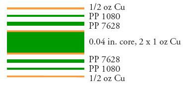
separately.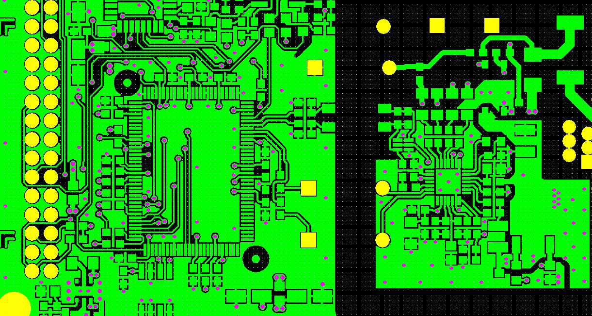 PCB specifications1. Multilayer 4 layer PCB2. Base material: FR-4 Tg135ºC3. Finished PCB thickness at 1.6mm +/-10% (1.62-1.68mm)4. Inner layer copper thickness 1oz (35um), Out layer copper thickness 1oz (35um)5. Green solder (Taiyo PSR-2000GT600D), White silkscreen (TAIYO IJR-4000 MW300)6. Surface finish: Immersion gold 2microinch 20%7. Finished PCB dimension: 214 mm x 276mm/8up8. Out layers
9. Applications:DSL Modems,ADSL Router,3G Modem,GSM Alarm,USB Dongle,WiFi USB Adapter,
WiFi Bridge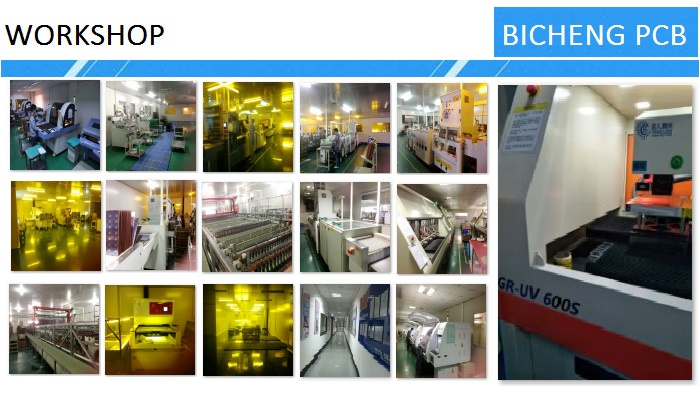
 Design For Manufacture
 | Serial NO. | Procedure | Item | Manufacturing capability |
Large volume
(S<100 m²) | Middle volume
(S<10 m²) | Prototype
(S<1m²) |
|
| 14 | Laminating | Tolerance of
laminate
thickness | ±10%
PCB thick | ±10%
PCB thick | ±8%
PCB thick |
| 15 | Maximum
laminate
thickness | 4.0mm | 6.0mm | 7.0mm |
| 16 | Laminate
alignment
accuracy | ≤±5 mil | ≤±4 mil | ≤±4 mil |
| 17 | Drill (18um,
35um,70um
etc are
finished
copper.
If not
mentioned
copper,
finished
1oz is the
default
value ) | Min.drill bit
diameter | 0.2 mm | 0.2 mm | 0.2 mm |
| 18 | Min.slot router
diameter | 0.60 mm | 0.60 mm | 0.60 mm |
| 19 | Min.tolerance of
PTH slots | ±0.15mm | ±0.15mm | ±0.1mm |
| 20 | Max.aspect
ratio | 1:08 | 1:12 | 1:12 |
| 21 | Hole tolerance | ±3mil | ±3mil | ±3mil |
| 22 | Space of via
to via | 6mil
(same net),
12mil
(different
net) | 6mil
(same net),
14mil
(different net) | 4mil
(same net),
12mil
(different
net) |
| 23 | Space of
component
hole to
component
hole | 12mil
(same net),
16mil
(different
net) | 12mil
(same net),
16mil
(different net) | 10mil
(same net),
14mil
(different
net) |
| 24 | Etching | Min.width of
etching logo | 10mil(18um),
12 mil (35um),
12 mil
(70um) | 8mil(18um),
10mil(35um),
12 mil(70um) | 6mil
(18um),
8 mil
(35um),
12mil
(70um) |
| 25 | Etch factor | 1.6-2.2 | 1.6-2.2 | 1.6-2.2 |
| 26 | Outer layer
(18um,35um,
70um etc
are finished
copper. If not
mentioned
copper,
finished 1oz
is the default
value ) | Min.via pad
diameter | 20mil | 16mil | 16mil |
| 27 | Min.BGA pad
diameter | 12mil | 12mil | 10mil |
| 28 | Min.track and
spacing | 5/5mil(18um) | 4/4mil(18um) | 3/3.5mil
(18um) |
| 5/5mil(35um) | 4/4mil(35um) | 3/4mil
(35um) |
| 7/9mil(70um) | 6/8mil
(70um) | 6/7mil
(70um) |
9/11mil
(105um) | 8/10mil
(105um) | 8/9mil
(105um) |
13/13mil
(140um) | 12/12mil
(140um) | 12/11mil
(140um) |
| 29 | Minimum grid | 10/10mil
(35um) | 8/8mil(35um) | 4/8mil
(35um) |
| 30 | Min.space
(conductor to
pad, pad to
pad) | 6mil(18um) | 5mil(18um) | 4mil
(18um) |
| 6mil(35um) | 5mil(35um) | 4mil
(35um) |
| 9mil(70um) | 8mil(70um) | 7mil
(70um) |
| 11mil(105um) | 10mil(105um) | 9mil
(105um) |
| 13mil(140um) | 12mil(140um) | 11mil
(140um) |
Learn and Buy PCB----PCB History
The creator of printed circuit board is Austrian engineer Paul Eisler. He invented the printed circuit
as part of a radio set while working in England around 1936. In 1943, The USA began to use the
technology on military radio. In 1948, the USA released the invention for commercial use. Since
the mid-1950s, printed circuits became commonplace in consumer electronics and began to be
widely used.
Before PCB, the interconnection between the electronic components is relying on the wires directly
connected to complete. Nowadays, only in the laboratory test wire exists. Printed circuit board in
the electronics industry has occupied the absolute control status.

Founded in 2003, Bicheng Enterprise Limited is a professional PCB export enterprise. We have established a good relationship of cooperation with well-known enterprises in the same industry.
The factories have been ISO 9001-2008, ISO 14001-2004 and ISO/TS16949-2009 quality management system certified. Over the past 14 years, we have provided professional circuit board manufacturing solutions for more than 5000 companies worldwide.
Different plant scale to suit for your requirements
16000 square meter factory building
30000 square meter month capability
8000 types of PCB per month
ISO9001, ISO14001, TS16949, UL Certified
We have our own advantages to help you saving cost and time spent on PCB, booster your new products go to market quickly.
A) Various kinds of PCB products
Double sided PCB
Multilayer PCB up to 32 layers
FR-4 PCB (Tg130, Tg170)
High frequency PCB (RO4350B, RO4003C)
Aluminum PCB (1W/MK, 2W/MK, 3W/MK)
Flexible PCB
HDI PCB Board
B) Multiple PCB technology to meet the market demands
Blind via PCB, Via in pad PCB, Fine pitch BGA PCB
Impedance controlled PCB
Heavy copper PCB
Hybrid material PCB
C) Many discount policies for new customers
SMT stencil foil, free of charge
Prototype shipping cost, free of charge
Prototype test, free of charge
PCB panelization, free of charge
D) High quality PCB services
Engineering design prevents problems from occurring in pre-production.
Meet your PCB needs from prototype to mass volume production.
Eligible products rate of first production: >95%
Delivery on time: >98%, door to door shipment service
Customer complaint rate: <1%
Choose BichengPCB means you choose hassle free.
More >
Other Products with This Manufacturers